

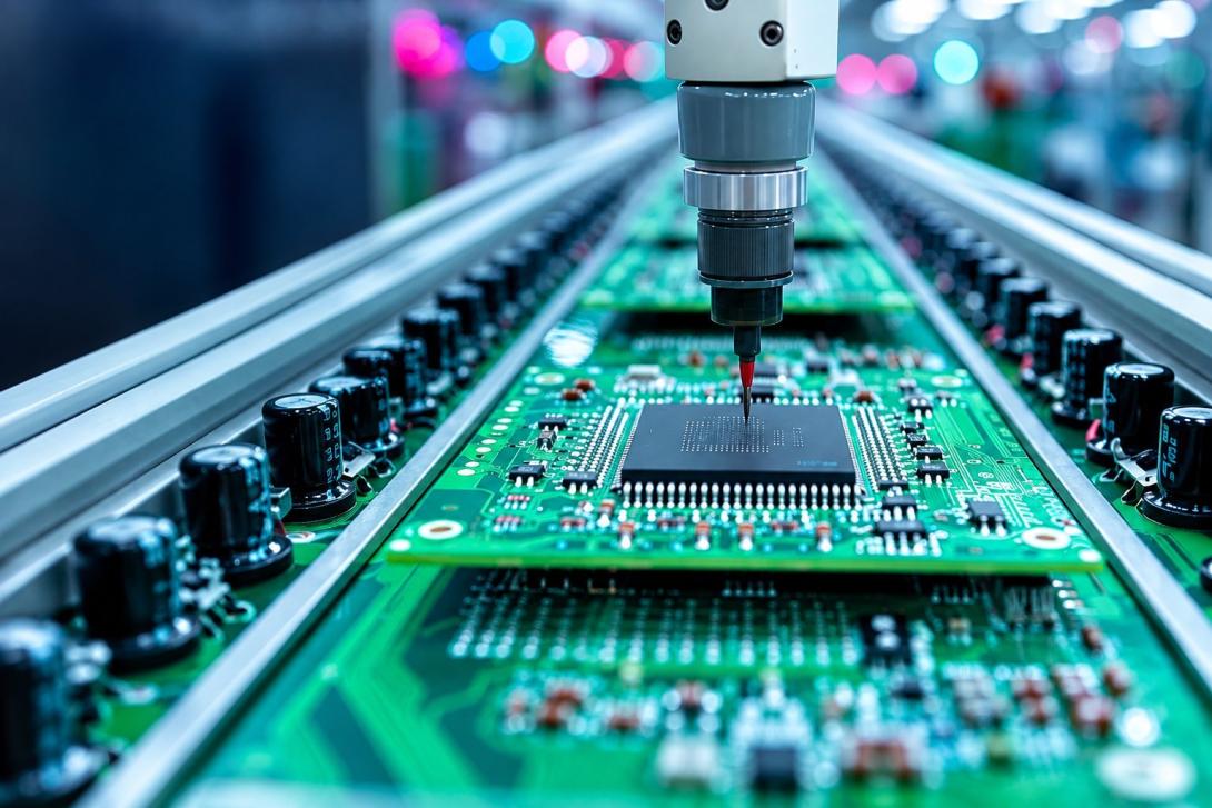
PCB manufacturing and assembly is the end-to-end process of transforming a circuit board design into a fully functional electronic product. It covers everything from fabricating the bare board to sourcing components, soldering, inspection, and functional testing. For OEMs and product developers, understanding each stage helps reduce errors, control costs, and accelerate time to market.
If you've ever wondered what happens between sending a Gerber file and receiving a finished, tested PCB this guide walks through the entire process without the fluff. Whether you're developing a new product or scaling an existing one, knowing how PCB manufacturing assembly works puts you in a stronger position at every stage.
What Is PCB Manufacturing and Assembly?
PCB manufacturing refers to the fabrication of the physical board the substrate, copper traces, drill holes, and surface finish. PCB assembly (PCBA) is what follows: placing and soldering electronic components onto that board to create a working circuit. Together, these two phases form the backbone of electronics production.
The distinction matters because they involve different equipment, lead times, and quality controls. A board can be perfectly fabricated but fail assembly if component placement or soldering parameters are off. Both phases need to work in sync.
Stage 1: Design Files and Pre-Production Review
Everything starts with your design files. Most manufacturers require a complete Gerber file package including copper layers, drill files, soldermask, silkscreen, and board outline. Alongside this, a Bill of Materials (BOM) and a pick-and-place file are essential for the assembly stage.
Before production begins, a competent manufacturer will conduct a Design for Manufacturability (DFM) review. This checks for issues like trace clearance violations, pad sizing errors, and component footprint mismatches that could cause failures downstream. Skipping this step is one of the most common causes of costly rework.
What Should Your DFM Review Cover?
- Minimum trace width and spacing compliance
- Drill-to-copper clearance
- Component pad compatibility with reflow or wave soldering profiles
- Panelization layout for efficient production
- Silkscreen clarity and reference designator placement
Stage 2: PCB Fabrication Building the Bare Board
PCB fabrication is a multi-step photochemical and mechanical process. It starts with a base laminate typically FR4 onto which copper layers are etched using a photolithographic process guided by your Gerber files.
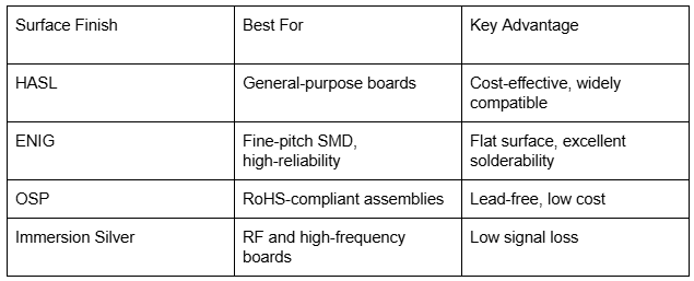
For multilayer boards, individual layers are bonded together under heat and pressure before drilling. Plated through-holes (PTH) are created by electroplating copper inside the drilled holes to allow electrical connections between layers. The board then receives a soldermask coating and surface finish common options include HASL, ENIG (Electroless Nickel Immersion Gold), and OSP.
Common PCB Surface Finishes Compared
Stage 3: Component Sourcing and Procurement
Once the bare boards are ready, attention shifts to components. This stage is often where lead times get unpredictable. Supply chain disruptions particularly relevant given recent global semiconductor shortages can delay even well-planned production runs.
Reputable PCBA manufacturing partners maintain relationships with authorised distributors and can flag long-lead-time parts early. They can also suggest approved alternative components (AVL Approved Vendor List) that meet your specifications without compromising performance. If you're sourcing components independently, make sure they come from authorised channels to avoid counterfeit parts, which remain a serious risk in the electronics supply chain.
Stage 4: PCB Assembly Where the Board Comes to Life
PCB assembly is where fabricated boards and components converge. The process differs depending on whether your design uses Surface Mount Technology (SMT), Through-Hole Technology (THT), or a mix of both.
SMT Assembly Process
SMT is the dominant method for modern electronics. The process follows a precise sequence:
- Solder Paste Application: A stainless steel stencil is aligned over the board, and solder paste is applied to pads using a squeegee.
- Component Placement: Pick-and-place machines position components at speeds of thousands of placements per hour with sub-millimetre accuracy.
- Reflow Soldering: The board passes through a reflow oven with a controlled thermal profile preheat, soak, reflow, and cooling zones melting and solidifying the solder joints.
Through-Hole Assembly
THT components are inserted manually or by automated insertion equipment and soldered using wave soldering. This method is still widely used for connectors, capacitors, and components that require mechanical strength or higher power handling.
Stage 5: Inspection Catching Defects Before They Become Problems
Inspection is not optional. It's the quality gate between production and delivery. In professional PCB production, multiple inspection methods are used at different stages.
- Automated Optical Inspection (AOI): High-resolution cameras scan the board post-reflow to check solder joint quality, component placement, and polarity. AOI can inspect thousands of points per second.
- X-Ray Inspection: Used for BGAs and QFNs where solder joints are hidden beneath the component body. X-ray reveals voids, bridging, and insufficient fill that AOI cannot detect.
- In-Circuit Testing (ICT): Electrical probes verify that each component is correctly placed and functioning within specified parameters.
According to IPC standards the global benchmark for PCB quality acceptable solder joint criteria are defined under IPC-A-610, the most widely referenced acceptance standard in the electronics manufacturing industry. Manufacturers certified to IPC-A-610 Class 2 or Class 3 offer verifiable quality levels suited to commercial and high-reliability applications respectively.
Stage 6: Functional Testing and Final Validation
Inspection checks for visible defects. Functional testing verifies that the assembled board actually does what it's supposed to do. This typically involves powering the board and running it through simulated operating conditions.
For complex products, this may include:
- Burn-in testing (extended operation to surface early failures)
- Environmental stress screening (temperature cycling, humidity exposure)
- Protocol communication testing (I2C, SPI, UART verification)
- End-of-line functional test fixtures designed around the specific product
This stage is especially critical for OEMs and product developers launching safety-critical or regulated products. In Singapore, electronic products sold or used in commercial and industrial environments may need to comply with standards governed by the Infocomm Media Development Authority (IMDA) and relevant IEC/EN standards for electromagnetic compatibility.
PCB Production Process: Prototype vs. Volume Production
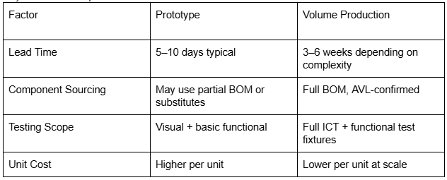
The PCB production process looks different depending on your volume. Prototyping prioritises speed and flexibility manufacturers may run small batches with manual handling and shorter lead times. Volume production prioritises consistency, yield optimisation, and cost efficiency through automation and process standardisation.
Key differences to plan for:
What to Look for in a PCB Manufacturing and Assembly Partner
Choosing the right manufacturing partner directly affects your product quality and launch timeline. Look for these indicators of a capable, trustworthy operation:
- IPC certification and documented quality management systems (ISO 9001 is a baseline)
- Transparent DFM review process before production starts
- Clear communication on lead times, component sourcing, and change management
- In-house AOI, X-ray, and functional test capabilities
- Experience with your specific product category or industry vertical
For OEMs and engineers in Singapore and the wider Southeast Asian region, working with a local partner also offers logistical advantages faster turnaround, easier site visits, and fewer cross-border compliance complications.
Statron offers end-to-end PCB manufacturing and assembly services in Singapore, supporting OEMs and product developers from design review through to final tested product. Their technical team works closely with clients at each stage of the PCB production process to ensure first-pass success and production-ready outcomes.
Frequently Asked Questions
What is the difference between PCB manufacturing and PCB assembly?
PCB manufacturing refers to fabricating the bare circuit board etching copper layers, drilling holes, and applying surface finishes. PCB assembly (PCBA) is the process of soldering components onto that board. Both stages are required to produce a fully functional electronic product, and each involves different equipment and quality controls.
How long does the PCB manufacturing and assembly process take?
Prototype runs typically take 5–15 business days from design file submission to completed PCBA. Volume production timelines vary based on board complexity, layer count, and component availability. Long-lead-time parts are the most common cause of delays, so early BOM review and sourcing are critical to staying on schedule.
What files do I need to submit for PCBA manufacturing?
You will need Gerber files for the board layers, a drill file, a Bill of Materials (BOM), a pick-and-place (centroid) file for SMT placement, and any special assembly or testing instructions. Providing complete, accurate files at the start reduces the risk of production delays and costly engineering queries.
What is a DFM review and why does it matter?
Design for Manufacturability (DFM) review is an analysis of your PCB design to identify features that could cause manufacturing defects or yield issues. It checks trace spacing, pad sizes, drill clearances, and panelisation layout. Addressing DFM issues before production starts avoids expensive rework and board respins later in the process.
What inspection methods are used in PCB assembly?
Professional PCB assembly lines use Automated Optical Inspection (AOI) to check solder joints and component placement, X-ray inspection for hidden joints under BGAs and QFNs, and In-Circuit Testing (ICT) to verify electrical performance. Together, these methods ensure defects are caught before boards are shipped or integrated into final products.
How do I choose between prototype and volume PCB production?
Prototype production suits design validation it is faster and more flexible but costs more per unit. Volume production is optimised for consistency and cost efficiency at scale, requiring fully confirmed BOMs and test fixtures. Most product development cycles start with prototypes and transition to volume production once the design is verified and stable.